Transmission electron microscopy (TEM)
Transmission electron microscopy
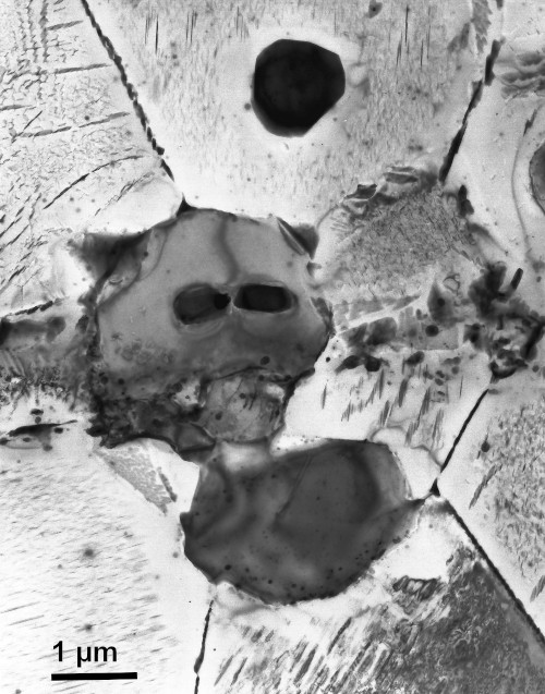
Transmission electron microscopy (TEM) is a microscopy technique in which a beam of electrons is transmitted through a specimen to form an image. The specimen is most often an ultrathin section less than 100 nm thick or a suspension on a grid. An image is formed from the interaction of the electrons with the sample as the beam is transmitted through the specimen. The image is then magnified and focused onto an imaging device, such as a fluorescent screen, a layer of photographic film, or a detector such as a scintillator attached to a charge-coupled device or a direct electron detector. Transmission electron microscopes are capable of imaging at a significantly higher resolution than light microscopes, owing to the smaller de Broglie wavelength of electrons. This enables the instrument to capture fine detail—even as small as a single column of atoms, which is thousands of times smaller than a resolvable object seen in a light microscope. Transmission electron microscopy is a major analytical method in the physical, chemical and biological sciences. TEMs find application in cancer research, virology, and materials science as well as pollution, nanotechnology and semiconductor research, but also in other fields such as paleontology and palynology. TEM instruments have multiple operating modes including conventional imaging, scanning TEM imaging (STEM), diffraction, spectroscopy, and combinations of these. Even within conventional imaging, there are many fundamentally different ways that contrast is produced, called "image contrast mechanisms". Contrast can arise from position-to-position differences in the thickness or density ("mass-thickness contrast"), atomic number ("Z contrast", referring to the common abbreviation Z for atomic number), crystal structure or orientation ("crystallographic contrast" or "diffraction contrast"), the slight quantum-mechanical phase shifts that individual atoms produce in electrons that pass through them ("phase contrast"), the energy lost by electrons on passing through the sample ("spectrum imaging") and more. Each mechanism tells the user a different kind of information, depending not only on the contrast mechanism but on how the microscope is used—the settings of lenses, apertures, and detectors. What this means is that a TEM is capable of returning an extraordinary variety of nanometer- and atomic-resolution information, in ideal cases revealing not only where all the atoms are but what kinds of atoms they are and how they are bonded to each other. For this reason TEM is regarded as an essential tool for nanoscience in both biological and materials fields. The first TEM was demonstrated by Max Knoll and Ernst Ruska in 1931, with this group developing the first TEM with resolution greater than that of light in 1933 and the first commercial TEM in 1939. In 1986, Ruska was awarded the Nobel Prize in physics for the development of transmission electron microscopy.
Read more about 'Transmission electron microscopy' at: WikipediaWikipedia contributors. "Transmission electron microscopy." Wikipedia, The Free Encyclopedia. Wikipedia, The Free Encyclopedia, April 20, 2024.
In transmission electron microscopy an electron beam is going through a very thin sample (usually < 100 nm thick). Due to the shorter wavelength of the electrons a far higher resolution can be obtained as compared to microscopy with light. TEMs can magnify objects up to 50 million times, and reach a maximum resolution of about 0.5Å
Based on the image contrast mechanisms, different properties of a sample can be investigated. Using TEM information e.g. about structure, crystallisation, morphology and stress of a sample can be obtained.
For TEM the sample must be thin enough to transmit sufficient electrons to form an image with minimum energy loss. Thus the careful preparation of the samples is a cruicial step in transmission electron microscopy.
The actual image - the micrograph - is obtained, by the electrons irradiating a phosphorescent screen, which emits photons, which again can be captured by film/CCD detector.
Resources used:
Department of Physics, Warwick, UK on TEM
See also:
KIT Laboratory for Electron Microscopy
HZDR Ion Beam Center - Structure Analysis
Other modalities related to Transmission electron microscopy in Helmholtz Imaging CONNECT:
In-situ and operando TEM provides a direct link between structural evolution and materials properties or function and the ability to identify transient structures, which cannot be observed ex-situ.
See also:
KIT on In situ EM